Hacking Furbo - A Hardware Research Project – Part 3: Chip Off and Persistence
In this third part of our Hacking Furbo blog series, we’ll focus on the Furbo hardware. We’ll detail our attempts to perform a chip off procedure to dump and re-apply our customized firmware. We’ll also discuss our struggles with the XGecu T48 programmer, the correct adapter, and our sad attempt at using a Probe Reader.
Introduction
In this third part of our Hacking Furbo blog series we will focus on the Furbo hardware; specifically our attempts at performing a chip off procedure on the device in order to dump and re-apply our own customized firmware. We will detail how we used the XGecu T48 programmer for the firmware extraction, our struggles to get the correct adapter, and our sad attempt at using a Probe Reader to avoid performing a chip off procedure.
While we hadn't performed a chip-off firmware extraction before, we had all the necessary tools to do so. For those following along at home these were:
- Hot air rework station
- Metal tweezers
- Flux pen with needle tip
- Adjustable clamp and board standoffs
- Solvent
- Flash programmer (XGecu T48)
However, the most critical tool we did not have at the time of starting this project was the adapter module that would allow us to dump and reprogram the flash chip using our programmer. We confirmed what was observed in the FCC ID application filing with a visual inspection once we had our first device. We were dealing with a WINBOND W25N02kV NAND Flash chip using the WSON8 6mmx8mm format.
After doing some research online we found a couple different adapter modules that could be used with our programmer in order to dump and reprogram this chip. We ordered a pair of modules from eBay and were looking at 3-4 weeks for shipping. And, in a tale as old as time, after 4 weeks had passed we noticed the tracking on our first order jumped from 3-4 weeks to 8-10 weeks. That was not an option so we went on the hunt for a new seller who could get us an adapter in the next couple of weeks. It was during this process we came across another type of device that could be used for reading and flashing these chips without having to remove them from their board—a flash probe. And so, in the hopes of speeding things up, we ordered one of these flash probes to see if it could work for what we needed in addition to another WSON8 6x8 adapter module.
Two short weeks later, our flash probe arrived from Australia and we got to work testing it on our devices. After many hours trying to get a successful read using the probe we were left with several corrupted reads and managed to brick our first Furbo device.
Not dissuaded by this, we decided to dig into why this was occurring and determine why our reads were failing. Our research revealed that the most common reason these probe reads fail is due to what is known as "Passive Drain", which is caused by the chip remaining on the board. In order to read from the chip, it must receive voltage, which is provided by the flash probe. However, when the programmer is sending voltage to the chip, other components on the board siphon that power enough to make the flash dump fail.
Unfortunately for us, this means that the only way to avoid these failures is by removing the chip from the board so that no voltage will be siphoned by other components. Said otherwise, we'd have to do a chip off firmware extraction—there was no getting around it. So that is what we did.
Chip Off Adventures
Eventually the second adapter module we ordered had arrived and it was time to attempt the chip removal.
We aligned the hot air stream over top of the chip and set the temperature to 725 degrees Fahrenheit. After a couple minutes had passed, we used the flux pen to apply a little bit of flux to both adjacent sides of the chip and watched it quickly get sucked underneath. Then, the solder went from having a dull matte finish to a shiny silver glaze—indicating that the solder may be liquefied. We lightly touched the chip with the tweezers and it moved! The solder had indeed liquefied, meaning all we had to do was carefully pick up the chip without disturbing any of the other components.
With great precision we managed to pick up the chip using the tweezers and removed it from the board. Phase 1 was complete, now for phase 2: reading the flash.

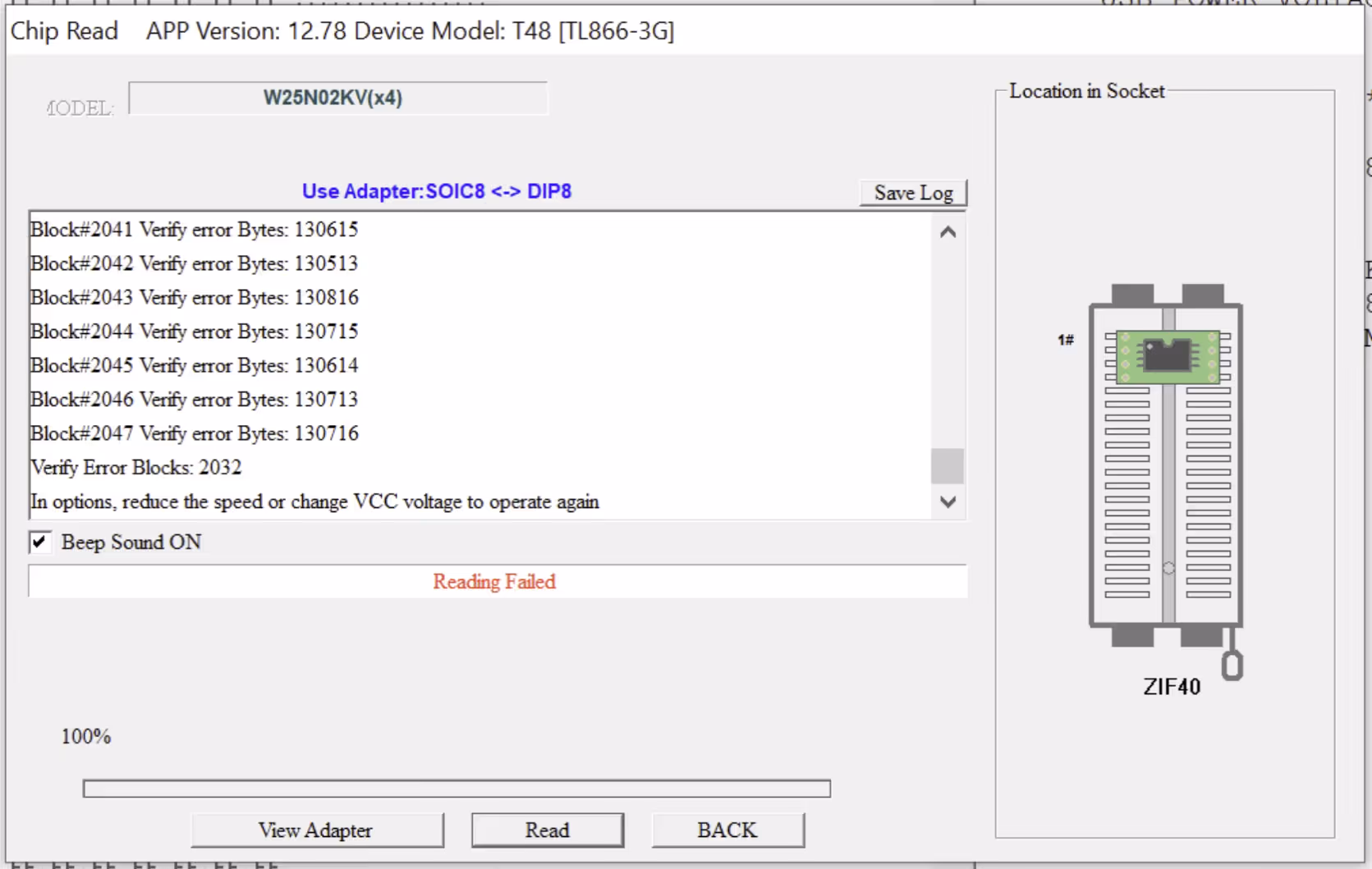
As this was our first time ever performing a chip off for a device it was also the first time using the XGecu programmer. We had a rough idea on what had to be done within the XGecu software to get a read from the chip based on our previous studying of Matt Brown's videos, but this turned out to be more challenging than expected.
Using our solvent we cleaned the flux residue left over on the chip, then inserted it in the adapter module, and started up the XGecu software to attempt to read the flash from the chip. We selected the chip model in the interface and confirmed all pins were connected properly.
“Success!”, we thought as the software returned a "Read Complete" message. We saved the dump to a .bin file and tried reading it with binwalk. Unfortunately the output seemed off, there was a ton of unknown data and when we attempted to carve out the file system and unsquash it we ran into corruption errors.
After several hours of trial and error, learning what each of these configuration parameters did, we found the missing link that had tripped us up so far. We had misconfigured two options on the software. These were:
- Customized NAND Parameters — Internal ECC: Enable
- Spare Area in the File — None: Enable
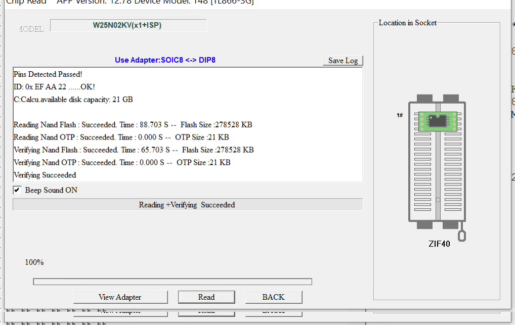
As the flash chip we were dealing with has ECC, that option needed to be enabled to properly read the chip. We also learned that the reason we had a bunch of null data in our dump was because we were also copying the spare area—unused space on the chip—from the flash into our binary. By disabling this setting and making sure ECC was being processed properly we were able to dump the contents of the NAND Flash and unsquash the file system. This meant we could finally proceed to phase 3: modifying the file system.

Persistence on the Device
By this stage of our research we had managed to crack the password hash for the root user of the device but we still wanted to change that password to something we controlled. We also wanted to add an easier shell to work from so that we did not require a disassembled camera and UART connection in order to login to the device. Since we knew the Furbo device was using DES for the password encryption, we simply encrypted our own password using DES and replaced the hash located in the /etc/shadow file.
Once this modification was made to the file system all that was left to do was repack the file system and splice it back into the original dump we had from the flash chip. We did this using mksquashfs and dd, similarly to how we carved out the file system originally and unpacked it using unsquashfs. Now that our modifications were added into the flash dump we could proceed to phase 4: reprogramming.
Reprogramming
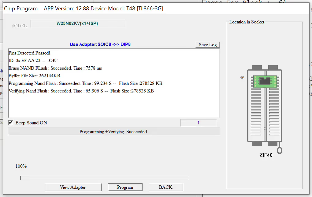
While we were learning about the configuration settings available in the XGecu platform to perform a successful read we also discovered what settings should be enabled for a successful write. The same options as before would be needed, as well as the enablement of the "Erase Before Programming" option so that the NAND Flash is always "zero'd out" before writing new data. It is also recommended to enable "Auto Verify after Read & Programming".
Loading the custom firmware into the XGecu platform is very straightforward, simply click Load, select the file format (which in our case was binary), and then select the buffer which for us was Flash Main Memory.
Once the custom firmware is loaded into the software you are ready to program the flash chip. After the programming was completed and the read check passed, we removed the flash chip from the adapter module and it was time for phase 5: re-soldering the chip to the board. This was by far the step we were most concerned about as improper installation could result in damage to the board or the flash chip.
Chip On Adventures
Rather than trying to add new solder to the board, we attempted to re-connect it with the residual solder and a bit of flux. Reheating the hot air rework station, we waited until the solder became liquefied on the board and then added a small dab of flux to the bottom of the flash chip. Using the metal tweezers we carefully moved the flash chip into position. After a short wait it seemed that the solder was united again; we could nudge the chip lightly back and forth to confirm all 8 leads were properly connected and had adequate solder around them.
We allowed the components to cool for a short while, and then it was time to see if we managed to rewrite the firmware and successfully mount this chip back onto the device. Thankfully, when we plugged in our UART cable and powered the device back on we were met with the familiar sight of UART logs. As we watched them fly by we tried logging into the device using our new password and... it worked! We successfully modified the root password for the device.
Conclusion
That concludes part three in this six-part blog series. Successfully performing our first ever chip off procedure in order to reset the root password on the device and establish persistence. Although we already had root access by this point, having cracked the password hash in part one, this procedure was still very important as it would allow us to modify other parts of the read-only file system that could not be modified previously. We would also end up using this method for analyzing differences between Subscription and Non-Subscription devices which would ultimately lead to the discovery of Unlimited Free Trial Licenses.
Chip-off analysis and firmware extraction are standard techniques in a thorough IoT security assessment. If an attacker can do it, so can a tester. If your device stores sensitive data in flash or relies on firmware integrity for security guarantees, IoT penetration testing will examine whether those guarantees hold up under physical access scenarios.
Ready to get in touch? Get started by booking a consultation now.
About the author

Julian B
Penetration Tester
Julian is an intermediate penetration tester with nearly five years of experience working in cybersecurity, dedicated to penetration testing, open-source intelligence gathering, and moving the needle forward for organizations across Canada. He regularly engages with the community through presentations at conferences, on a range of topics including vulnerability research and OSINT investigations. This is work is underlined by several CVEs which have been attributed to his research on open-source applications.

.avif)